Let Istar help you get started on your project with our experience and know-how!
Upload your design files and production requirements and we will get back to you within 30 minutes!
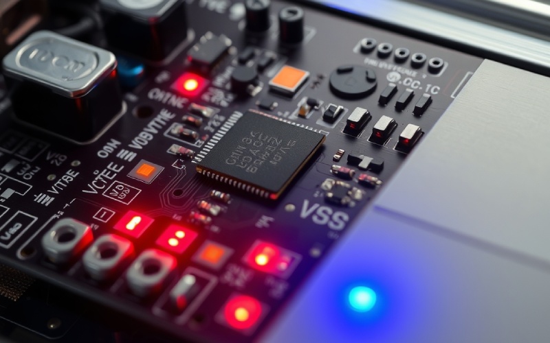
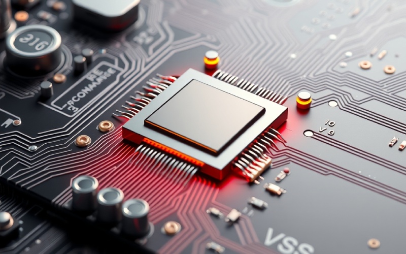
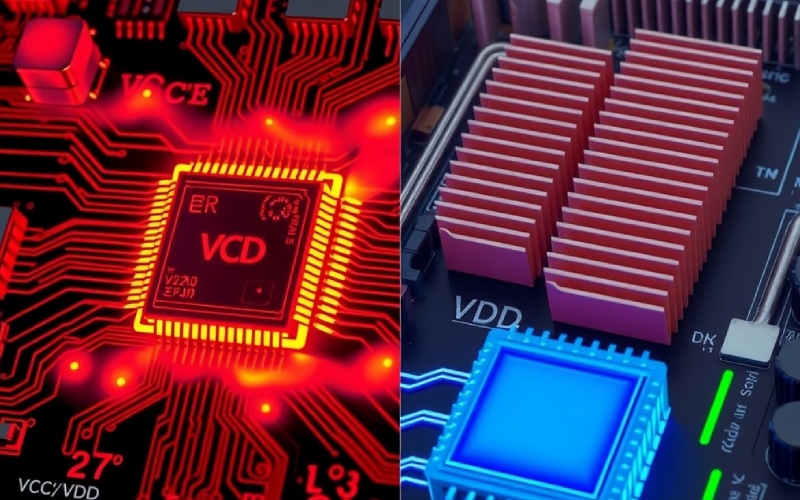
You’ve seen the jumble of letters for power supplies on drawings and circuit boards (PCBs): VCC, VDD, VEE, VSS. What is the difference between VCC and VDD? Are VSS and GND the same? It’s a classic example of technical words making things hard to understand. I’m here to show you that it’s not as confusing as it looks. In this article, I’ll explain these terms in simple English, using my own experiences. We’ll look at the history behind the names and, more importantly, I’ll give you the practical know-how to understand exactly what kind of power supply voltage a part needs. When you finish reading, you’ll be able to look at datasheets and circuit drawings with confidence, which will make you a better and more informed engineer or hobbyist. This isn’t just about learning facts; it’s about building a strong base for your work in electronic circuits.
Let’s start by figuring out what the letters mean. In electronics, ‘V’ almost always means voltage. The two letters that come after, though, can be a little more puzzling. The “CC” in VCC points to the collector part of a Bipolar Junction Transistor (BJT). So, VCC is the positive supply voltage that goes to the collector of a BJT. This term became the standard when bipolar transistors were the main technology used.
In the same way, the “DD” in VDD points to the drain part of a Field-Effect Transistor (FET). So, VDD is the positive supply voltage that goes to the drain of a FET. As FETs, especially in CMOS technology, became more common, VDD became the standard term for the main positive voltage in those circuits. So, you can see the pattern: the name is directly linked to the kind of transistor technology used in the circuit. The meaning of vcc is connected to the collector voltage. I will use the term vcc many times since it is the main topic. The term vdd is also a big part of this talk.
People often ask me why we use “VCC” or “VDD” and not just “VC” or “VD”. The reason is a simple but important rule. The single letter, like ‘C’ for collector or ‘D’ for drain, usually means the voltage at that one part compared to ground. The double letter, “CC” or “DD,” means it is the supply voltage for the whole circuit or a part of it. The vcc is the supply voltage.
This small change in how it’s written means a lot. It helps engineers quickly tell the difference between a measurement at one spot and the main power line that feeds many parts. For instance, the voltage at the collector of one transistor might change while the circuit is working, but the VCC supply voltage should stay the same. This rule helps prevent confusion in a circuit diagram. So, VCC is usually understood to be the main positive voltage source for a part of the circuit. The working voltage of the chip is often shown by VDD. Using two letters helps tell the difference between the power supply voltage and the voltage at a certain spot on the transistor.
This is the most important part. The main difference between VCC and VDD is the kind of technology they are connected with.
I’ve dealt with plenty of both bipolar and CMOS designs, and remembering this difference is very important. While both VCC and VDD give a positive voltage, knowing which term to find on a datasheet tells you right away what kind of parts are inside. For example, if I see VCC pins on an IC, I can guess it’s probably a bipolar device. If I see VDD, I’m almost sure I’m looking at a CMOS device. The working voltage of the chip is a key detail. Using vcc and vdd helps tell the two types of technologies apart. The power supplies for these devices are a main part of the circuit design.
| Feature | VCC | VDD |
|---|---|---|
| Connected Technology | Bipolar Junction Transistors (BJT) | Field-Effect Transistors (FET), CMOS |
| Stands For | Voltage at the Collector | Voltage at the Drain |
| Common Use | TTL Logic, Analog Amplifiers | Microcontrollers, CPUs, Digital Logic |
Now that we understand VCC and VDD, let’s add their partners, VEE and VSS, to the discussion. Just like VCC and VDD are usually positive power supplies, VEE and VSS are usually the negative or ground connections. The pattern is the same as before.
The “EE” in VEE stands for the emitter part of a BJT. In many analog circuits, especially amplifiers, you’ll find a dual power supply with both a positive and a negative supply. In these situations, VCC would be the positive voltage and VEE would be the negative voltage. This lets the output of the amplifier go both above and below ground. The emitter voltage is measured from VEE.
In the same way, the “SS” in VSS stands for the source part of a Field Effect Transistor. For a digital circuit, which usually runs on a single power supply, VSS is normally connected to the ground (0V) point. VSS is the lowest voltage in the circuit, which in most digital systems is ground. So, vss is the source. You’ll often find vdd and vss together in datasheets for cmos circuits. The terms vee and vss are needed to understand the whole power supply setup. The vss is the negative supply in many situations.
This is a question I’m asked frequently, and it’s a good one. In many, if not most, digital circuits, VSS is, in fact, connected to the ground terminal (GND). For a simple circuit getting power from a battery or other power source, VSS and GND are basically the same point, acting as the 0V reference for the whole system.
But it’s not always so simple. The important thing is that VSS specifically means the lowest voltage level connected to the source part of the FETs inside an IC. GND is a broader term for the reference point that all other voltages are measured from. In some complex systems, you might have several “ground” levels. For instance, you could have separate analog ground and digital ground areas on a PCB to keep noisy digital parts away from sensitive analog circuits. In that case, VSS for a digital IC would connect to the digital ground. The key thing to remember is that even though VSS is often connected to GND, the term VSS is specifically about the power supply connections of an IC. We also have ac ground in some systems.
To really get these ideas, it’s helpful to know how a transistor works. Think of a transistor like an electronic switch or valve. The supply voltage gives the power for this valve to operate. In an NPN bipolar transistor, VCC gives the positive voltage to the collector. A small current at the base lets a much bigger current flow from the collector to the emitter, which makes the signal stronger or turns a load on or off. The vcc is the positive supply that allows this. The collector voltage is a key detail in this action.
In a MOSFET, the idea is similar but the science is different. VDD gives the positive voltage to the drain. A voltage at the gate controls how much current flows from the drain to the source. The vdd is the working voltage that lets the MOSFET turn on and off. The connection between drain and vss is very important for how the device works. The field-effect transistors are controlled by this voltage. The drain voltage is a key part of how a MOSFET works. Both bipolar transistor and MOSFET devices need these power supplies to work right. The NPN transistor is a frequent type of bipolar transistor. The vcc and vdd terms are key to understanding how they work. The vee and vss terms set the lower voltage line.
Of course! I’ve worked on many designs where this happens. These are often known as mixed-signal circuits because they have both analog (often bipolar) and digital (CMOS) parts on the same circuit board. For example, you could have a sensor with an analog amplifier (needing VCC and maybe VEE) sending its signal to a microcontroller (which needs VDD and VSS).
In these cases, it’s very important to have a well-made power network. You have to make sure that both the VCC and VDD power supplies are clean and steady. Often, ICs with both analog and digital parts will have separate power pins (like VCCA for analog VCC and VCCD for digital VCC) to help with this. Some new ICs have both vdd and vcc pins, but this is not as common. The main thing is to look at the datasheet for the power needs of each part. Having both vcc and vdd on the same board means you need to plan carefully. The terminals of the device must be hooked up to the right voltage.
When you have a mix of analog and digital parts, the ground connection becomes very important. Digital circuits, especially fast ones, can create a lot of noise on the ground line. This noise can cause a lot of problems for sensitive analog circuits, like an amplifier.
To stop this, designers often make separate ground connections for an analog ground (AGND) and a digital ground (DGND). The VSS of the digital ICs would connect to the digital ground, while the ground point for the analog parts would connect to the analog ground. These two ground areas are then usually connected at one single spot, often close to where the power comes in. This method stops the digital noise from messing up the analog signals. Sometimes, you might also find a shielding ground used to block noise. The idea of ground and signal ground is key to good circuit design. The common ground terminal is where these different grounds are often joined.
This is where you put knowledge into practice. The datasheet is your greatest resource for finding out the power needs of a part. Here is my process:
The datasheet will clearly state the needed supply voltage of the circuit. It might also list an IO voltage for the input/output pins, which can sometimes be different from the main VDD voltage.
You can have a perfect drawing, but if your PCB layout is bad, your circuit might not work right. The paths that VCC and VSS follow on the printed circuit boards are very important. The higher voltage of vcc needs to be routed with care.
I always suggest using power planes on a PCB with multiple layers. This involves setting aside a whole layer of copper for VCC and another for GND (which is linked to VSS). This gives a path with low resistance for the current, which is needed for things to work steadily. It’s also very important to put decoupling capacitors as near as possible to the VCC and VSS pins of every IC. These capacitors are like tiny, local pools of charge, giving the IC the quick bits of current it needs and cleaning up noise on the power supply voltage. A good layout for the power supply voltage is a sign of a professional design. The link between vcc and vss is basic.
Even though the different names for power supplies in electronics can look confusing at first, they have a clear pattern based on the technology they use. By knowing the history and uses of VCC, VDD, VEE, and VSS, you can look at any circuit diagram or datasheet with confidence.
Here are the key things to remember: