Let Istar help you get started on your project with our experience and know-how!
Upload your design files and production requirements and we will get back to you within 30 minutes!
Upload your design files and production requirements and we will get back to you within 30 minutes!
Semiconductor CNC machining is the specialized process of creating ultra-precise parts for the chip manufacturing industry. At Istar Machining, we use advanced computer-controlled machines to make the critical components needed in semiconductor fabrication equipment.
These parts must meet extremely tight tolerances and be made from special materials that won’t contaminate the sensitive chip-making process. Our work helps make the microprocessors, memory chips, and sensors that power your everyday devices like phones and computers.
Supports uploading of the following file formats: .STEP .STP .SLDPRT .STL .IPT .3MF .3DXML .PRT .SAT .DXF .X_T .X_B .JT .CATPART
Istar Machining's years in the industry
The size of Istar Machining's factory
Our CNC equipment count
Istar's number of skilled machinists/operators


Our precision CNC machining services for semiconductor applications offer:
Material Type | Common Uses | Special Properties |
Silicon & Germanium | Wafer carriers, test fixtures | Semiconductor-grade purity, brittle |
Ceramics (AlN, Al₂O₃) | Plasma chambers, gas injectors | High temperature resistance, non-conductive |
Stainless Steel 316L | Vacuum components, flanges | Ultra-clean, non-magnetic options |
High-purity Plastics | Chemical delivery, wafer handlers | Particle-free, chemical resistant |
Specialty Alloys | RF components, thermal parts | Low thermal expansion, high conductivity |
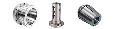
Our CNC machining service creates many critical semiconductor components:
In semiconductor manufacturing, even the tiniest speck of dust can ruin an entire wafer of chips. That’s why precision isn’t just important—it’s absolutely necessary.
Our 5-axis machining capabilities let us create complex shapes with perfect accuracy. When making parts for plasma etch chambers, we need to achieve tolerances of ±0.001mm—that’s about 1/50th the width of a human hair! These tight tolerances ensure:
At Istar Machining, we use multiple advanced processes to create semiconductor components:
Our 5-axis machines can create complex 3D shapes in a single setup, maintaining tight tolerances throughout. This is perfect for making electrostatic chuck components that need perfectly flat surfaces with intricate cooling channels underneath.
For extremely precise cuts in hard materials, we use EDM machining (Electrical Discharge Machining). This process can cut through materials like tungsten with accuracy down to 0.0001 inches.
Our CNC turning services create perfectly cylindrical parts used in vacuum systems and gas delivery components.
When components need perfect flatness, our surface grinding services can achieve surface variations of less than 0.0001 inches across an entire part.
Every semiconductor part we make goes through strict quality checks:
Our semiconductor CNC machining work helps create:
Parameter | Typical Specification | Our Capability |
Tolerances | ±0.001mm (0.00004″) | ✓ Achieved with precision equipment |
Surface Finish | Ra <0.2μm | ✓ Mirror-like finishes standard |
Cleanroom Standard | ISO Class 7 | ✓ Dedicated clean manufacturing area |
Material Purity | Semiconductor grade | ✓ Certified material sources |
Lead Time (Prototypes) | 5-15 days | ✓ Quick-turn options available |
When you work with Istar Machining for your semiconductor parts, you get:
A leading semiconductor equipment manufacturer needed custom gas distribution plates for their new etching system. These complex parts required:
Our team used CNC milling to create the base shape, EDM for the precise hole pattern, and worked with specialized coating partners for the plasma-resistant finish. The final parts were delivered on time and performed flawlessly in the customer’s system.
While semiconductor is our specialty, our precision machining capabilities serve many high-tech fields:
Ready to discuss your semiconductor component needs? Contact Istar Machining today:
For vacuum applications, we typically recommend 316L stainless steel, aluminum 6061-T6, or specialty alloys like Kovar that have been properly cleaned and prepared for high-vacuum environments.
Our semiconductor components are processed in an ISO Class 7 cleanroom environment and undergo special cleaning steps to remove all traces of machining oils, particles, and contaminants.
Yes, we can machine base components from resistant materials like alumina ceramic, or apply specialized coatings like yttrium oxide (Y₂O₃) that withstand harsh plasma environments.
Prototype parts can be ready in 5-15 days depending on complexity. Production runs typically require 2-4 weeks, but we offer expedited services when needed.
Yes, we provide full material certifications and traceability documentation for all semiconductor components.